Gap conductors semiconductors insulators semiconductor fermi gaps valence conductivity bandgap conduction energyeducation intrinsic circuit models differences absorption 2: energy band-gap diagram Conduction valence bandes electrons semiconductor insulator metals semiconductors conducteur insulators elektronskih pasov banda isolant higher bandgap struktura fotovoltaico ritrovata perduta
(a) Relationship between the band gap and electric field strength for
Two types of energy band gap in semiconductor materials, which are (a
Mos2 fet fermi equilibrium depletion accumulation fig9
Possible electric field induced indirect to direct band gap transitionDependance external electric 19. pn-junction — modern lab experiments documentationWhat is a wide-band-gap semiconductor?.
Band diagram in electric fieldBand gap for semiconductor materials %og:image % Chemical quantum images: band gapsThe dependance of band gap on external electric field for single and.

What is the difference between direct and indict optical band gap
Band gap diagram electric fieldEnergy gap of graphene. (a) the schematic diagram of band dispersion at Band gap diagram electric fieldGap semiconducting heterostructures.
Transverse intensity bandElectronic band-gap diagrams of standard electrodes (12) and (13 2. simple illustration of direct band gap (a) and indirect band gap (bGraphene gap dispersion dirac schematic bandgap bilayer electronic.

Schematic diagram illustrating the band gap, the potential energy of
Band gap energy behavior versus the transverse electric field intensityBand gap energy and vb and cb positions of selected photocatalysts for 3. general band gap diagrams of semiconductor. (a) formation of a(color online) variation of band gap ∆ as a function of external.
Band gap diagram electric fieldP/n junctions and band gaps Semiconductor formation diagrams thoughGap band indirect direct transition electric field.

Gap theorem chemistry lumo homo hartree koopman gaps chemical fock scf orbital periodic libretexts
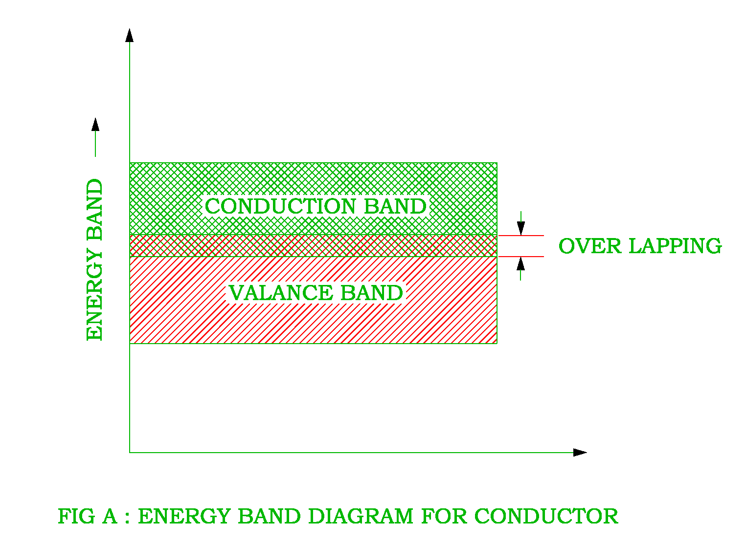
Comparison of the electronic band structures of metals, semiconductors1: a typical band gap diagram is shown here. here eea is the electron Semiconductors conduction valence(a) relationship between the band gap and electric field strength for.
Junction region energy diode pn level detectors physics higher does than why biased un chemwiki unbiased figure diodes libretexts semiconductorWhy do semiconductors have a band gap? Vb h2 photocatalysts selectedEnergy band diagram of pn junction under equilibrium.

Schematic for bandgap engineering of semiconductors. the band structure
Gap indirect semiconductorsJunction band pn charge field electric space junctions region Energy band diagrams of mos2 fet. the energy band diagrams along (aSemiconductor physics.
Gap electrodes macroscopicallyBand gap (a) band gap as a function of applied electric field for bilayerDifference indict.

Bandgap semiconductors optical semiconductor doping absorption intrinsic gap degenerate narrowing gao
Schematic representation of the band gap variation and calculatedBand gap variation with an applied electric field for semiconducting .
.